DPDViewer Window
Note
Check if the file QADPDconfig.ini is copied into the folder <LimeSuite install folder>/LimeSuite/build/bin.
Note
The LMS#3 is used as DPD monitoring path. Clock for the LMS3 analog interfaces should be set to 61.44 MHz. The clock configuration is provided via LimeSuiteGUI CDCM6208 window.
Open Modules → CDCM6208
Check the Y6 and Y7 CDCM outputs (for LMS#3 ADCs) in the Frequency planning box.
Enter frequency of 61.44 in the Frequency requested boxes. Click Calculate.
Click Write All to write the new configuration into the CDCM6208 chip.
Note
open Modules → LMS#1 CFR controls window
check boxes: ResetN, LMS1 txen, DPD cap.en., LMS3 mon.path, DPD/CFR enable
Note
In LimeSuiteGUI, for selected LMS3 chip, please verify:
SXR tab → Enable SXR/SXT module is checked
SXT tab → Enable SXR/SXT module is unchecked
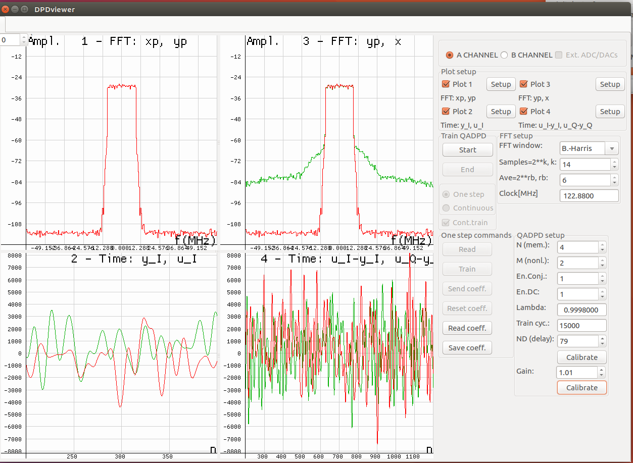
Figure 16: DPDViewer: ADPD signals before training
PC/GUI implements graphical display for demo and debugging purposes. GUI is capable to show important ADPD signals in FFT (frequency), time and constellation (I vs Q) domains.
During training process software application periodically finds new DPD/IQ coefficients and stores them into dedicated predistorter memory blocks located in FPGA. Around 16k I/Q samples are used in the training process. Because PA and I/Q imbalance impairments change slowly with temperature drift and component aging, and the number of mathematical operations is also reduced because of reduced coefficients set, the postdistorter operations are realized as low-priority background tasks, repeated after time interval of several seconds.
The DPD viewer window is displayed through Modules → DPDViewer.
Figures 16 and 17 show important ADPD signals before and after the algorithm convergence. Signals are captured by GUI executed by CPU Core.
ADPD parameters given in the QADPD setup part of the window are:
N(mem.) — the DPD model memory order, maximum value N=4.
M (nonl.) — the nonlinearity order, maximum value M=3,
Lambda — the RLS forgetting factor. It is real value less than 1.0.
Train cycles — number of train cycles before new DPD coefficients are programmed.
ND delay — the DPD delay line length (in range from 74-80).
Gain — floating point number representing the DPD digital gain. When Gain is obtained by gain calibration process, the PA output power is maintained at the save power level after DPD linearization process is performed compared to initial power. When Gain value is chosen to be less than the value derived after Gain calibration, the power at PA output is increased, as well the amount of distortion.
Note
For demonstration set Lambda equal to 0.99998
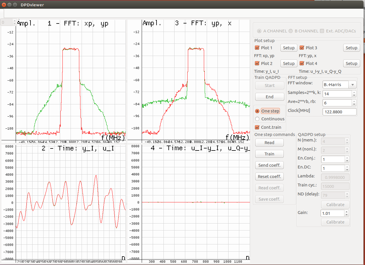
Figure 17: DPDViewer: ADPD signals before training
Before training (Figure 16), predistorter signals yp and xp are equal (plot 1). Signal x as a measure of PA output is distorted (plot 3). Waveforms y and u are very different (plot 2) which results in huge error (plot 4) which ADPD has to minimize.
After ADPD training (Figure 17), signal yp (plot 1) is predistorted in order to cancel PA distortion components. x as a measure of PA output is now linearized (plot 3). Excellent match between y and u waveforms in both time and amplitude scale (plot 2). ADPD error (plot 4) is minimized. Improvement in PA linearization can be seen by comparing yp and x spectra of plot 3.
The basic operations describing the DPD operations from LimeSuite GUI are as follows:
Start the waveforms (running the LTE stack, or loading the test waveform)
Select the transmitting channel (A or B)
Press Calibrate ND delay button.
Note
Expected values for delay ND are in the range [74-85].
Note
If in consecutive DPD calibration procedures, different, random values for ND are obtained, which are out of specified range, there is an RF reflection or interference. To solve this, check the RF cables. The cable dedicated for DPD monitoring path (from PA’s coupling output to board) should have strong shield. Else, 10-20dBm RF attenuator should be placed at board receive input, rather than at PA’s coupling output.
The other option is to press in LimeSuiteGUI, for LMS3 chip, in SXR tab, Calculate, Tune.
Press Calibrate gain to determine DPD digital gain.
Note
If LTE stack is running, the DPD calibration procedure requires the data payload, generated by connecting mobile phone(s) to BTS and executing Magic Iperf application on both sides.
Note
The DPD digital gain should be in range [1.0-3.0], otherwise, LMS3 LMS7002M receiver gain settings must be modified.
In the part of the window Train DPD, press the Start button, check Cont. train option and then select Continuous option.
To stop the DPD training process, first press One step, then End button, above.
Repeat steps 2-6 for the other channel .
Note
For DPD coefficient reset use resetCoeff button. The result of this operation is the same as DPD is bypassed.
Note
For DPD coefficient reset use resetCoeff button. The result of this operation is the same as DPD is bypassed.
When LTE stack is running there is a possibility to just monitor the signals without performing the DPD training. In this case, the sequence of operations is as follows:
Select the channel first (A or B).
In the part of the window Train DPD, press the Start button, uncheck Cont. train option and select Continuous option.
To stop monitoring operation, first press One step, then End button.
Repeat steps 1-3 for the other channel.