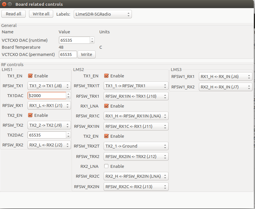
The board LimeSDR-PCIe-5G incorporates three LMS7002M ICs, named with LMS1, LMS2, LMS3.
For DPD demonstration the LMS1 and LMS3 are used. Two transmitter channels (named with channels A and B) are implemented by LMS1.
The DPD monitoring paths are realized by two LMS3 receiver paths. The pre-driver TQM8M9079 PAs
are embedded on the board, located in LMS1 transmit paths.
The LMS2 is used for 5G signal transmission and implements two transceiver chains.
Moreover, the LMS2 TX chain includes the CFR block, specifically optimized for 100 MHz bandwidth waveforms.
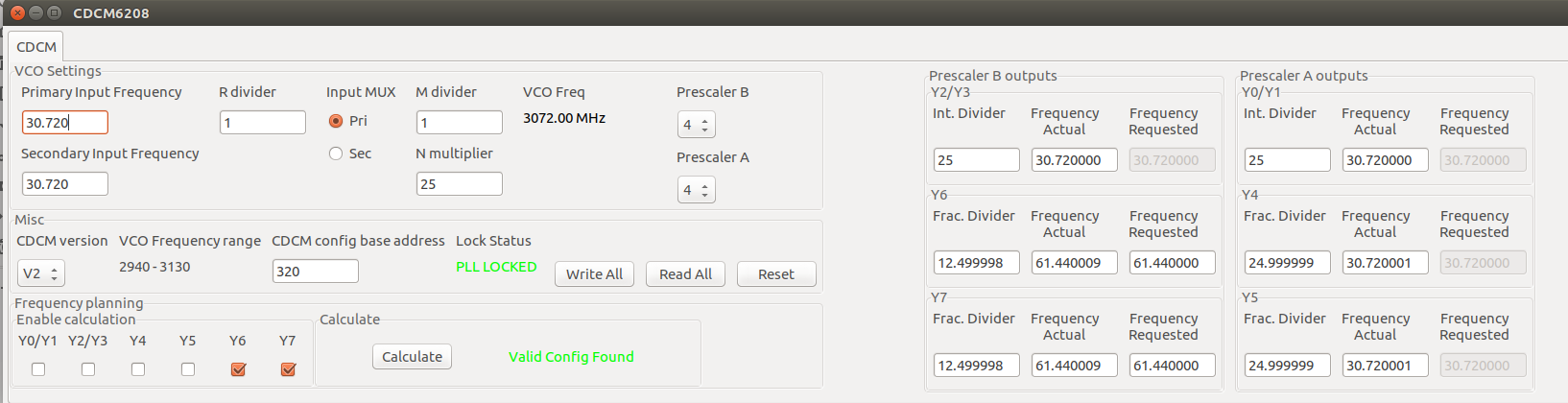
Clocks for the LMS2 and LMS3 analog interfaces are provided by the onboard CDCM6208 clock generator.
Whenever it is required to change the frequency value of on-board DAC and ADC, please follow:
Open Modules → CDCM6208.
Check the Yi CDCM outputs in the Frequency planning box.
Then, enter desired frequency in the Frequency requested box.
Click Calculate. If a valid configuration is found, the text Valid Config Found appears.
Then, click Write All to write the new configuration into the CDCM6208 chip.
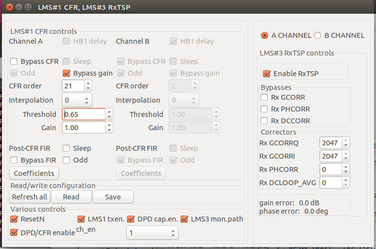
The radio buttons A_CHANNEL and B_CHANNEL select one of the TX paths: A or B (Figure 13).
Two CFR blocks and accompanying post-CFR FIR filters are implemented in transmit
paths A and B. Before any modification of CFR parameters is made, the
TX path must be selected using the previously specified radio buttons.
The CFR processes the LTE signals which data rate depends on signal bandwidth.
For 5MHz and 10MHz bandwidths it is 30.72MS/s; for 15MHz and 20MHz the rate is 61.44MS/s.
The data processing rate is changed via Interpolation option.
CFR parameters for each of the TX paths include:
Bypass CFR – when is checked, the CFR is bypassed.
Interpolation option has possible values 0 and 1 (Figure 13). The value 1 selects the
interpolation in front of CFR block. (see Figure 6). In this case the data rate
of signals entering the LMS1 CFR block is 61.44 MS/s. Otherwise, when 0 value is chosen,
the interpolation is used after CFR and post-CFR FIR blocks. In this case the
data rate of signals is 30.72 MS/s.
CFR order is the integer value representing the CFR PWFIR order. When
Interpolation = 0 the CFR order maximum is 40; When control signal
Interpolation = 1, maximum PWFIR order is 20.
Threshold is the floating point number in the range from 0.0 to 1.0,
determining the clipping threshold. The value is normalized to input signal
amplitude maximum. The parameter Threshold determines the amount of PAPR
reduction. For example, the value of 0.707 reduces the input signal PAPR by 3dB.
When value of 1.0 is chosen, the clipping operation is bypassed.
Gain is the digital gain following CFR block. The default value is set to 1.0.
The low-pass FIR filter follows the CFR block (Figure 6). The options for
FIR filter coefficients reading end programming are provided.
When Coefficients button is pressed, the post-CFR FIR filter coefficients
are read from FPGA registers and displayed in the new window.
New FIR coefficients can be loaded from .fir file and displayed in the window.
After pressing OK button, the window is closed and new coefficients are programmed
into the FPGA registers.
The FIR is bypassed when Bypass FIR is checked.
Note
Since distinct post-CFR FIR filters exist in
A and B channels, it is required to select the transmitting channel before
changing FIR coefficients. For this purpose the radio buttons A_CHANNEL/B_CHANNEL are used.
Note
For different LTE waveforms (5MHz, 10MHz, 15MHz and 20MHz) the corresponding
The coefficient values, stored in the .fir file, are derived after normalized FIR filter
coefficient values are multiplied with constant integer number of 215-1.
To save or read FPGA configuration the window (Figure 13) provides three buttons:
Refresh all button reads the configuration which has been already programmed
in the FPGA and updates the configuration in the window.
Read button which reads the .ini2 file, updates the configuration shown in
the window and also, automatically programs the FPGA registers.
The configuration includes all settings which are shown in the window,
including the CFR and post-CFR FIR coefficients for both channels.
Save button is used to read the configuration from FPGA and save it into the .ini2 file.
Additional controls:
ResetN - used for debugging purposes, should be always checked
LMS1 txen - used for debugging purposes, should be always checked
DPD cap.en. - when checked, the captured signals are sent to DPDViewer instead of FFTViewer.
When DPD is used should be always checked.
LMS3 mon.path - specifies the DPD monitoring path, when checked, the LMS3 receiver
is used, otherwise it is the LMS1 receiver. By default should be checked.
DPD/CFR enable - should be checked whenever CFR and DPD operations are required.
When unchecked, DPD/CFR operation is bypassed.
Note
When LMS1 DPD & CFR are used, the DPD cap.en. is checked.
When LMS2 Equaliser is being calibrated, the DPD cap.en. must be unchecked.
At right side, the window provides bypass check boxes and value editing fields for the
following LMS3 RX static corrector modules:
Phase I/Q imbalance correction (Rx PHCORR)
Gain I/Q imbalance correction (Rx GCORRI and Rx GCORRQ)
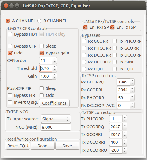
The radio buttons A_CHANNEL and B_CHANNEL select one of the LMS2 TX paths: A or
B (Figure 14).
The data rate of signals is 122.88MS/s or 245.76 MS/s.
The data processing rate can be changed via Interpolation option specified by Bypass HB1.
The Bypass HB1 should be unchecked and 245.76 MS/s used.
LMS2 CFR parameters for each of the TX paths include:
Bypass HB1, when checked, the interpolation is skipped (Figure 7). In this
case, the data rate of signals is 122.88 MS/s. When Bypass HB1 is left unchecked (in this case HB1 delay must be checked),
the data rate of the signals, which are processed by CFR, is 245.76 MS/s.
Bypass CFR – when is checked, the CFR is bypassed.
CFR order is the integer value representing the CFR PWFIR order.
The CFR order maximum is 32;
Threshold is the floating point number in the range from 0.0 to 1.0,
determining the clipping threshold value, normalized to signal
full-scale. For example, the value of 0.707 reduces the input signal PAPR by 3dB.
When value of 1.0 is chosen, the clipping operation is bypassed.
Gain is the digital gain following CFR block. The default value is set to 1.0.
Note
Interpolation require that HB1 Bypass is unchecked and HB1 delay is checked.
The LMS2 low-pass post-CFR FIR filter follows the CFR block. By pressing the button Coefficients,
the FIR coefficients are read from FPGA registers and displayed.
Also, new coefficients can be loaded from .fir file and displayed.
After pressing OK button and new coefficients are programmed into FPGA.
Option Bypass FIR bypasses the post-CFR FIR operation.
Option TX input source selects the NCO signal or regularly transmitted waveform.
At right side of the window, the window provides bypass check boxes and value editing fields for
various LMS2 RX and TX static corrector modules:
Phase I/Q correction (PHCORR)
Gain I/Q correction (GCORR)
I and Q components DC offset correction (DCCORRI and DCCORRQ)
Note
The coefficients for 100MHz Low-Pass FIR are provided by
The filter has 32 taps and the same number of coefficients.
The coefficient values are derived after normalized coefficient values are multiplied
with a constant 215-1.
Additional buttons are provided:
Button ResetEQU, which resets the LMS2 Equaliser (the effect is that the Equaliser is bypassed).
Button Read reads the .ini2 file, updates the configuration shown in
the window and also, automatically programs the FPGA registers.
The configuration includes all settings which are shown in the window,
including the CFR, post-CFR FIR and Equaliser coefficients for both A and B transmitting channels.
Save button is used to read the configuration from FPGA and save it into the .ini2 file.