Crest Factor Reduction (CFR)
Motivation for Peak to Average Power Ratio Reduction
Modern modulation schemes (LTE, 5G NR and similar) generate signals which inherently contain frequent and large peaks in time domain. In the presence of high Peak to Average Power Ratio (PAPR), PAs must be heavily backed off and/or further linearized by DPD. The efficiency of DPD algorithms themselves is also affected by high PAPR.
The solution which helps DPD to compensate PA distortions more efficiently is to deal with the signals with reduced PAPR. In this case, it is possible to increase transmitted signal average power, avoid PA operation in non-linear region and consequently improve PA energy and spectral efficiency.
The utilization of PAPR reduction techniques in modern telecommunication systems becomes a “must have” option, at least at BTS side.
NOTE: Peak to Average Power Ratio Reduction (PAPR) is also known as Crest Factor Reduction (CFR). The Crest Factor Ratio (CFR) is defined as a ratio between the signal magnitude maximum value and the signal average value:
Peak to Average Power Ratio (PAPR) is defined as:
Peak Windowing Method
Hard Clipping (HC) technique cuts the peaks when the envelope |x(n)| of the complex signal x(n) exceeds user selectable threshold level Th:
HC is quite simple. However, it produces high signal distortion due to hard clipping. Undesirable side effects of HC include in-band signal distortion which is measured by Error Vector Magnitude (EVM) and out-band signal distortion, measured by Adjacent Channel Power Ratio (ACPR). For that reason, we have adopted Peak Windowing (PW) algorithm for PAPR reduction. In PW, the large signal peaks are multiplied with a windowing function to smooth the sharp edges at clipping points. In fact, the above clipping coefficients c(n) are replaced by b(n):
where w(n) is some symmetrical windowing function (Hann’s for example).
The difference between c(n) and b(n) is minimized by choosing narrow window lengths which results in lower EVM degradation. However, if clipping operation happens frequently, neighboring correction windows overlap and the difference between c(n) and b(n) becomes larger.
For LTE standards, usually 30.72 MS/s sample rate is used. CFR block itself runs at 122.88 MHz clock frequency, i.e. four times the data rate in order to bust hardware DSP blocks processing power. Of course, these frequencies can easily be changed to conform to any other similar telecommunication standard.
The implementation of PW consists of several stages. The PW processing operations are depicted in Figure 3.a.
To determine the envelope e(n)=|x(n)|, complex I/Q input components are squared, summed and square-rooted. The envelope e(n) is then compared to the threshold level Th.
If the magnitude of e(n) is greater than threshold Th, clipping coefficient c(n) is calculated as the value of Th divided by e(n). Otherwise, c(n) value is set to one.
Peak search block is introduced in PW processing stage to find local minimum values of the signal c(n). If the input sample is not local minimum, then the output of Peak search block (signal cp(n)) is set to one.
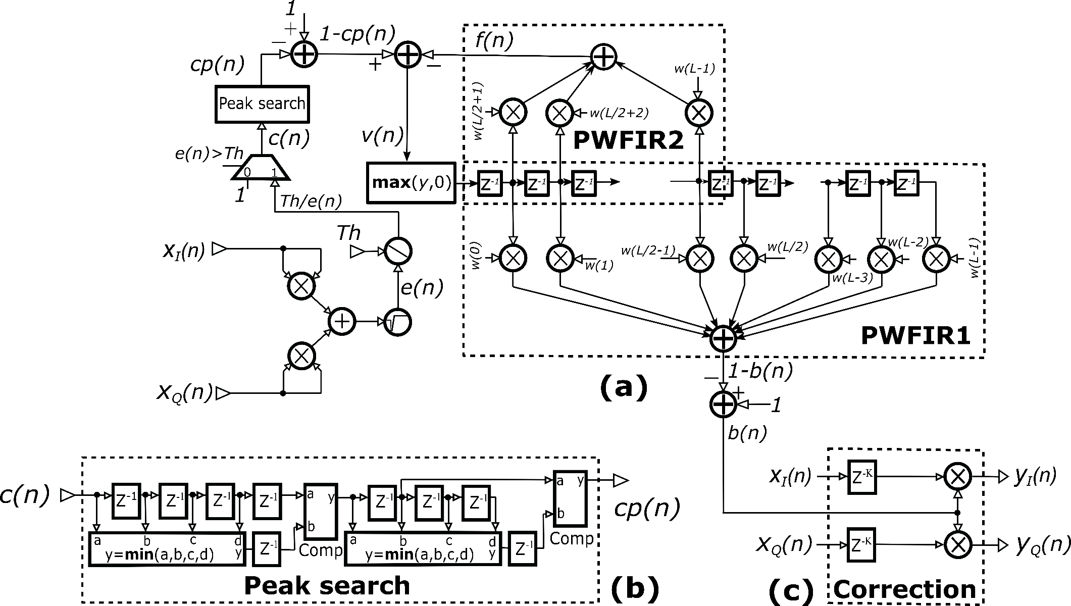
Figure 3: (a) Peak windowing architecture (b) Peak search block and (c) Correction block.
Figure 3.a shows the architecture of PWFIR filter. PWFIR consists of feed-forward (PWFIR1) and feedback (PWFIR2) sub-filters.
PWFIR takes input signal v(n) and generates 1-b(n). Negative values of v(n) are replaced by zeros before driving the rest of the filter. The sequence b(n) is gain correction of the input sequences xI(n) and xQ(n).
Prior to applying the correction, xI(n) and xQ(n) are properly delayed compensating for the delay (latency) introduced by the implementation of PWFIR and other CFR preprocessing stages. Hence, CFR output y(n) is constructed as shown in Figure 3.c.
In order to reduce overlapping, the feedback structure (PWFIR2) is introduced. The feedback path adjusts the next filter input value. Looking forward to when clipped input value reaches the center tap (Figure 3.a), the contribution of all previous input values (between first and center tap) are calculated and used for correction of the next input value. At the time when incoming clipped signal reaches the unity weighted center tap, the contributions from all previous values have already been compensated. This reduces the EVM degradation when successive peaks in cp(n) occur within the period shorter than half of the window length.
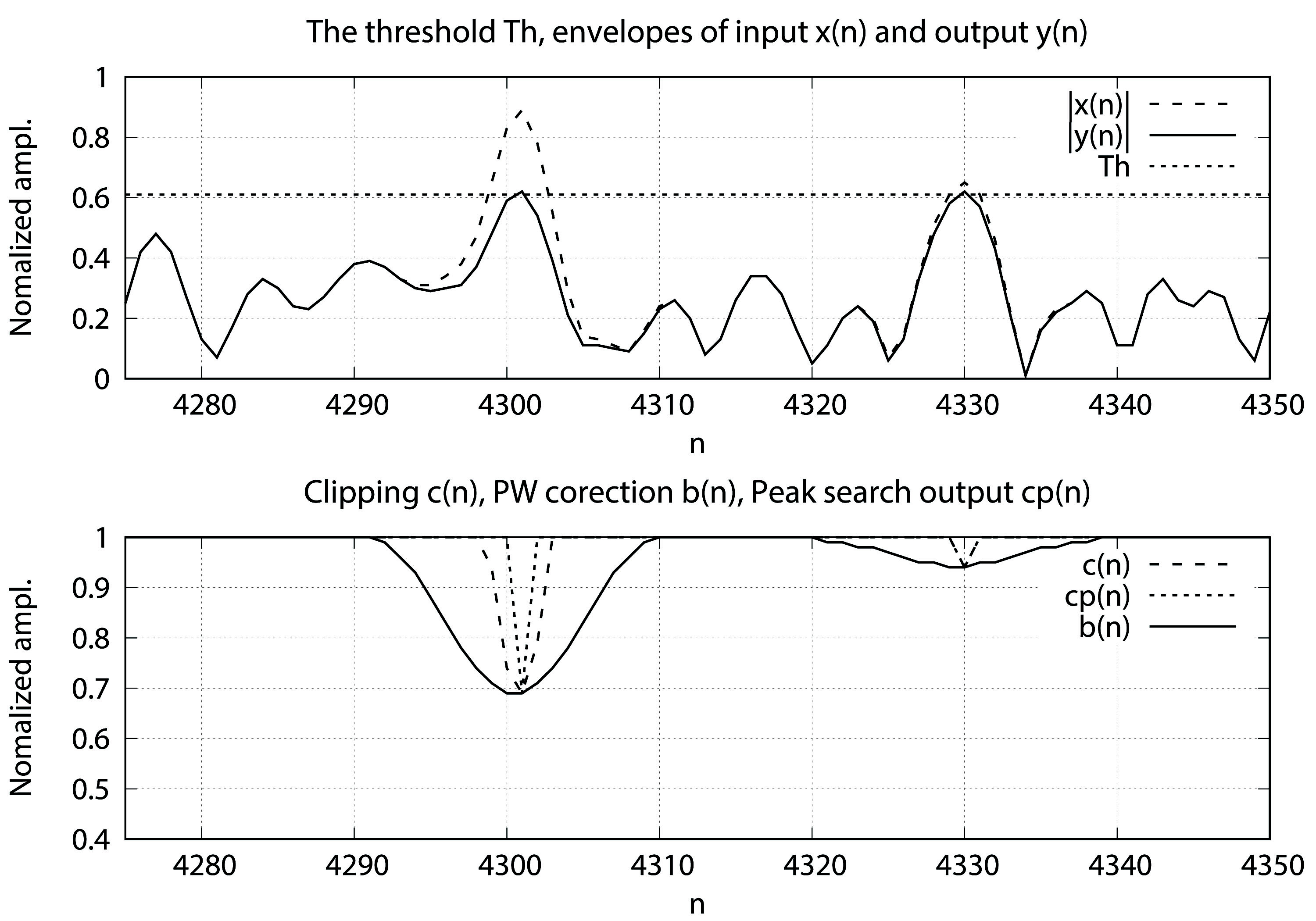
Figure 4: CFR algorithm in action. Bottom graph gives c(n), cp(n) and b(n), top graph shows Th, e(n) =|x(n)| and envelope of the CFR output |y(n)|.
As mentioned before, PWFIR filter structure is divided into two parts. PWFIR1 produces output signal 1-b(n) while PWFIR2 generates the feedback signal f(n) (Figure 3.a). For the implementation, we have chosen Hann windowing function:
PWFIR is designed to implement 1 ≤ L ≤ 40 tap filters where the filter length L and the filter coefficients w(k) are easily software programmable.
The architecture of PWFIR filter is based on multiply-and-accumulate (MAC) circuitry.
The architecture is area optimized. The number of utilized multipliers is reduced by multiplexing input data and operating the block at the clock frequency which is four times higher than the sample rate. PWFIR operates at the clock frequency of 122.88 MHz while input and output data rates are both equal to 30.72 MS/s.
The architecture of CFR FIR filter is further optimized by exploiting the fact that the filter has symmetrical window coefficients. The required number of multiplications is reduces by factor of 1/2. Consequentially, the number of FPGA DSP blocks used for the filter implementation is also reduced.
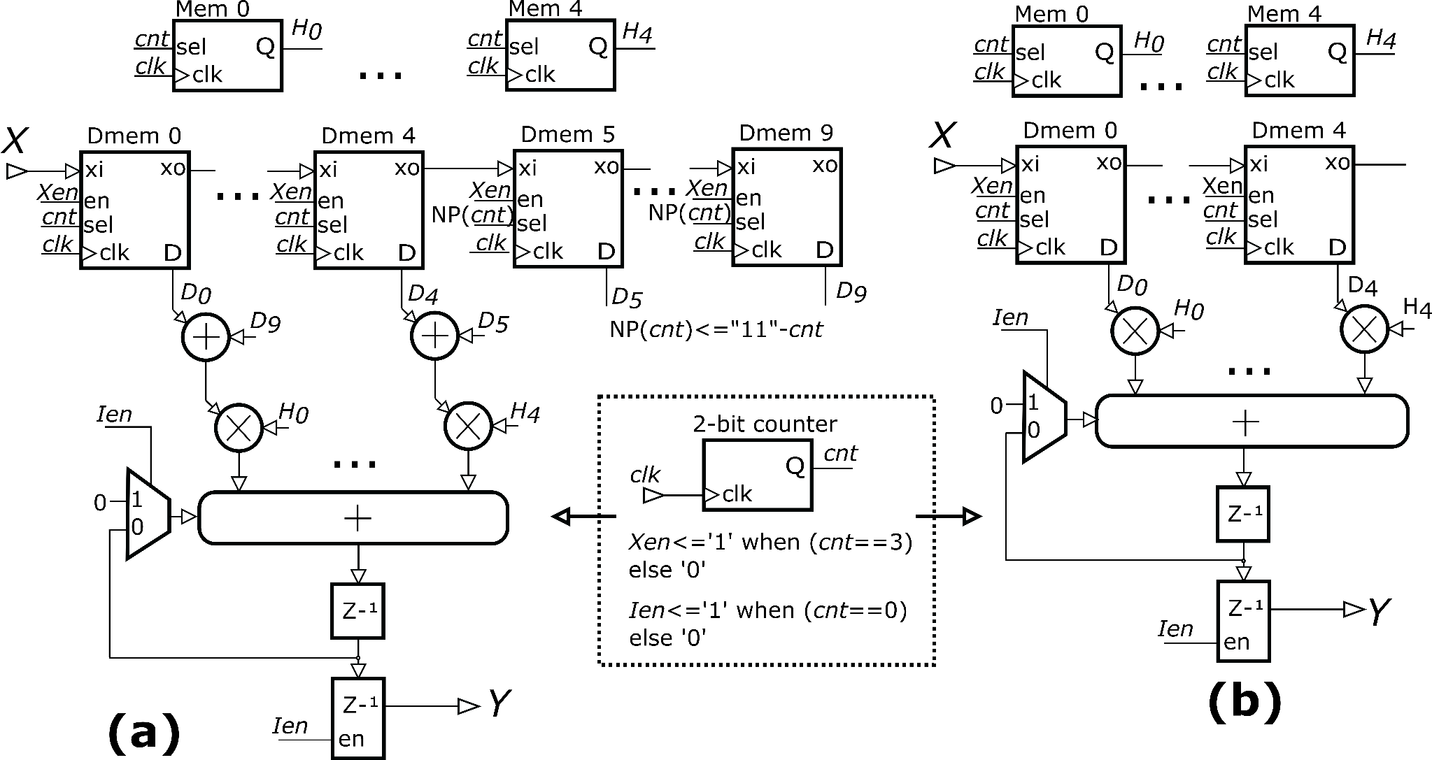
Figure 5: The architecture of PWFIR1 (a) and PWFIR2 (b) modules.
The detailed architecture of PWFIR1 is given in Figure 5.a. The coefficients are indexed from 0 to 19. Whenever the condition is true, the coefficient at index j is determined by following equation. Otherwise, the coefficient is set to zero.
PWFIR2 architecture is given in Figure 5.b. It provides up to 20 programmable filter coefficients which are stored in the register array and indexed from 0 to 19. The coefficients of PWFIR2 are determined by following equation whenever condition is met. Otherwise, the coefficient value at index j is set to zero.