LimeSDR-PCIe-5G Implementation
LMS1 transmit path
Note
LimeADPD I/Q algorithm is implemented via the LimeSDR-PCIe-5G board
LimeSDR-PCIe-5G incorporates three transceiver LMS7002M chips, named with LMS1, LMS2, LMS3.
LMS1 is dedicated to 4G LTE signal transmission and LimeADPD I/Q is implemented in its transmit path.
Two transmitter channels, named with channels A and B, are implemented by LMS1.
The board integrates TQM8M9079 power amplifiers — which are employed for DPD demonstration — in LMS1 transmit paths.
LMS3 is used to implement DPD monitoring paths.
LimeADPD I/Q and CFR algorithms were implemented using LimeSDR-PCIe-5G board, a high level block diagram of which is shown in Figure 6. For clarity, Figure shows the minimum hardware options required to illustrate the LimeADPD I/Q algorithm.
The digital circuits implementing LimeADPD I/Q operate at 122.88 MHz clock, while its input/output sample rates are 61.44 MS/s. Interpolation block is used to double usual LTE sample rate of 30.72 MS/s before driving DPD block. A DPD sample rate of 61.44 MS/s (or higher) is required if we want to cancel at least IMD3 products in the case of 20 MHz modulation.
The pre-distorter implementation in FPGA is optimized by multiplexing input data. Namely, the pre-distorter operates at a clock frequency which is two times greater than the data processing rate.

Figure 6: LimeADPD I/Q implementation based on LimeSDR-PCIe-5G board.
As shown in Figure 6, frequency conversion from BB to RF is performed by LMS1 transmitter chains. Frequency down-conversion from RF to BB, which is required for DPD monitoring path implementation, is performed by LMS3 receive chains.
The pre-distorter, ADCs and DACs operate at a rate of 61.44 MHz.The internal LMS7002M on-chip 12-bit DACs are used. The data rate at the LimeLight interface is 61.44 MS/s. At the LMS3 receiver side, the chip-external (on-board) 14-bit AD converters are used.
In order to increase the capacity of the radio link, 2x2 MIMO transceiver is implemented using LMS1 IC. In each of the transmit channels, separate DPD, CFR and low-pass FIR filter blocks were implemented. The LMS1 receive channels are not used for DPD, they are part of 2x2 MIMO receiver.
The CFR block has provision for changing the number of FIR filter taps L in the range 1 ≤ L ≤ 40. The 40-tap PWCFR module operates at 122.88 MHz clock frequency. The clipping threshold can be set to 0 ≤ Th ≤ 1. The threshold is floating point number. The value of 0 is equivalent to “CFR power down” while 1 corresponds to “CFR bypass”.
CFR output is filtered by on-FPGA digital low-pass post-CFR FIR filters (Figure 6). These filters are very frequency selective and efficiently remove out-of-band unwanted products generated by BB digital modem, as well as CFR PW method itself.
The interpolation/decimation option can be enabled or disabled. The choice is related to the modulation bandwidth as shown later.
If the interpolation control signal is zero (see Figure 6), the data rate of CFR input signal samples which come (from WFM RAM) to CFR input, is 30.72 MS/s. Therefore, the PWCFR operates at the clock frequency level which is 4 times greater than processing data rate. In this case, the data interpolation (using up-conversion of factor of 2) is used after CFR and post-CFR FIR blocks (see Figure 6). The number of taps in these filters is 40. The order L is in the range 1 ≤ L ≤ 40.
If the interpolation control signal is equal to one (Figure 6), interpolation (using up-conversion of factor of 2) is used in front of CFR and post CFR FIR blocks. (see Figure 6). In this case, the data rate of signals processed by CFR and post-CFR FIR blocks is equal to 61.44 MS/s. Therefore, the PWCFR operates at the clock frequency level which is only 2 times greater than processing data rate. The data interpolation, located after the CFR and post-CFR FIR blocks, is now bypassed. The number of taps in the CFR and post-CFR low-pass filters is limited to 20. Therefore, the L is in the range 1 ≤ L ≤ 20.
LMS2 transmit path
Note
The CFR algorithm is implemented in LimeSDR-PCIe-5G board LMS2 TX paths.
LMS2 is dedicated to 5G signal transmission, having greater bandwidth.
Two 2x2 MIMO transmitter channels, named with channels A and B, are implemented by LMS2.
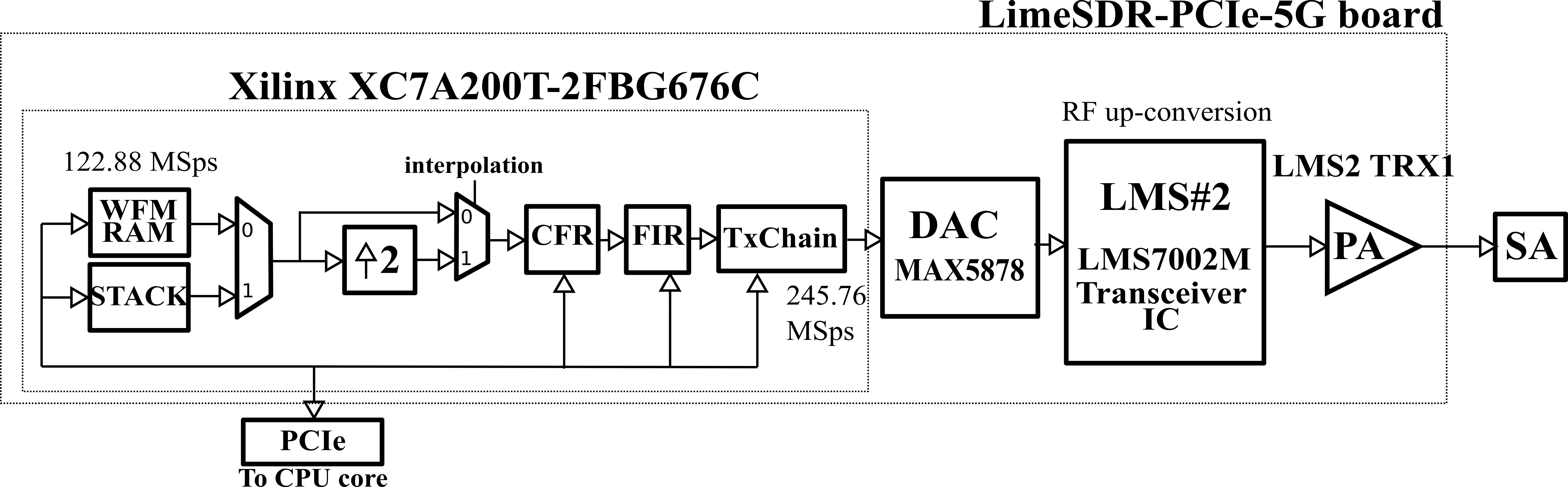
Figure 7: CFR implementation in LMS2 path of LimeSDR-PCIe-5G board.
The BB digital modem is implemented by host software which generates waveforms at rate of 122.88 MS/s. The waveforms are fed to the SDR board through PCIe interface.
The CFR and FIR are implemented in the FPGA. The CFR is based on the Peak Windowing technique.
The interpolation/decimation option can be enabled or disabled. The choice is related to the modulation bandwidth. An oversampling of factor one is used before the CFR block, yielding a maximum data rate of 245.76 MS/s,
The interpolation block is required in order to eliminate unwanted DAC-related signal images in the output signal at antenna point, in the case when signal bandwidth is wide, as it is case with 5G signals.
The interpolation block which doubles the usual 5G signal sample rate of 122.88 MS/s before driving CFR block is specifically designed for 100 MHz bandwidth signals.
The CFR digital circuits, incorporated in LMS2 transmit path, operate at 245.76 MHz clock signal, while its input/output sample rate is also 245.76 MS/s. The CFR block has provision of changing the number of FIR filter taps (L) in the range 1 ≤ L ≤ 32. Besides, the clipping threshold can be set to 0 ≤ Th ≤ 1.
The CFR output is filtered by low-pass post-CFR FIR filters (Figure 7). FIR filter is used to eliminate spectrum re-growth produced by BB modem and CFR. The number of taps in post-CFR low-pass filters is limited to 32. The FIR circuits operate at 245.76 MHz clock rate.
As shown in Figure 7, frequency conversion from BB to RF is performed by LMS2 LMS7002M transmitter chains. The RFIC-external on-board 16-bit DACs are used and the data rate is 245.76 MS/s.
The 2x2 MIMO transceiver is implemented using LimeSDR-PCIe-5G board LMS2 IC. In each LMS2 TX channel, separate interpolation block, CFR and low-pass FIR filter blocks are included.
Equaliser implementation
The Equaliser implementation can be divided into the hardware and software parts. The hardware part of Equaliser, realized by FIR filters, is implemented on LimeSDR-PCIe-5G board, in LMS2 transmit and receive paths.
Regarding data converters, external, on-board DACs and ADCs are used. Frequency conversion from BB to RF is performed by LMS2 transmitter chains. Frequency down conversion from RF to BB is implemented by LMS2 receive chain.
Separate FIR filters (EQUI, EQUQ) process transmitter and receiver I and Q signal components. Therefore, in a single transceiver chain four FIR filters are implemented. For both TX and RX signal paths, Equalisers are implemented as 16-tap FIR filters.

Figure 8: Transmit chain Equaliser architecture.

Figure 9: Receive chain Equaliser architecture.
The software part, which is specifically designed for LimeSDR-PCIe-5G board, is implemented by software application. Main parts of software application are:
receiver and transmitter calibration routines,
the coefficient’s calculation, and,
coefficients programming operations.
The first part of the application implements the LMS2 receiver and transmitter calibration operations, and consists of three phases designated as Phases 1, 2 and 3. They are described in details as follows:
The LMS3 RX I/Q imbalance measurement (Phase 1)
In Phase 1, the LMS2 performs the transmitter operation and the LMS3 is a receiver.
First, the LMS3 receiver DC is calibrated.
Then, the LMS3 receiver IQ imbalance is measured. The LMS3 RX LO is set to target TX LO frequency; the LMS2 TX NCO is enabled and BB frequency is set to 0MHz; the test signal is generated by LMS2 TXLO, which is changed in order to generate the signal tones at different frequencies. The LMS2 TXLO is swept in the range LMS3 RX LO -/+ 50MHz.
Amplitude, gain and phase error values are calculated from FFT of the data, which is captured by LMS3 RX.
The LMS3 RX IQ imbalance codes for different BB frequencies are obtained as the outputs of Phase 1.
The LMS2 TX IQ imbalance measurement (Phase 2)
LMS2 is transmitter, LMS3 performs a role of receiver in Phase 2.
The LMS2 transmitter DC is calibrated.
The LMS2 TX LO is set to target TX LO frequency; the LMS3 RX LO is also set to target TX LO frequency.
The LMS2 TX IQ imbalance is measured, the LMS2 TX NCO is swept in the range -/+ 50MHz.
The LMS3 RX IQ imbalance codes, which are obtained in the Phase 1, are used in the Phase 2.
Amplitude, gain and phase error values are calculated from FFT of the captured LMS3 RX output data.
The LMS2 TX IQ imbalance codes are obtained as outputs of Phase 2.
The LMS2 RX IQ imbalance measurement (Phase 3)
LMS3 is transmitter, LMS2 is receiver.
LMS3 TX LO = LMS2 RX LO = Target LO frequency.
LMS2 receiver DC is calibrated.
The LMS2 receiver IQ imbalance is measured. The LMS2 RX LO is set to target LO frequency; the LMS3 TX LO is changed in order to generate signal tones. The LMS3 TX LO is swept in the range LMS2 RX LO -/+ 50MHz.
Amplitude, gain and phase error are calculated from FFT of captured LMS2 RX data.
The LMS2 RX IQ imbalance codes are obtained as the outputs of Phase 3.
The receiver and transmitter calibration routines produce, after all three phases are completed, give the gain gm(x), the IQ gain error gerr(x) and IQ phase error \({\phi}\)err(x).
The results from calibration phases are then used for the calculation of TX and RX FIR Equaliser coefficients, as described in the chapter Mathematical Background of the Equaliser Design Procedure.
The results of the second part of the application are the coefficients for EQUI and EQUQ FIR filters. Finally, the coefficients are programmed into the EQUI and EQUQ hardware which is realized in FPGA.